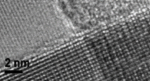
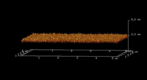
中文 / EN
OUR PRODUCTS
  • X-ray silicon nitride membrane

    Biologicalsample support membrane in STXM technology

    MORE
  • TEM silicon nitride membrane

    TEM sampler holder support membrane

    MORE
  • Nano porous silicon nitride membrane

    Apply tolong sequence, low cost, single molecule high throughput DNA sequencing technology.

    MORE
  • In situ liquid chip

    Real-time dynamic observation of nano_samples in liquid environment.

    MORE
  • Customized service

    Customized MEMS technology solution achievemore RD innovation.

    MORE
  • products advantages
  • Super clean

    Clear imaging

    100-level clean environment preparation

    100% inspection

  • High strength

    Super support

    Pressure tolerance (PSI): 60

    Stress: 250Mpa

  • Super flat

    Surface roughness: <0.3nm

    Thickness consistency: <5%


  • Piece by piece inspection

    Mature technology

    Piece by piece inspection

    Quality assurance

  • Scientific Research Case
  • High Transparency and Strength: Silicon Nitride X-ray Windows for Precise Radiation Analysis

    X-ray windows are specialized thin film materials used in X-ray analysis systems. Their primary function is to allow X-rays to pass through and interact with the sample while isolating the vacuum environment from the sample's atmosphere. X-ray windows are commonly used in X-ray spectroscopy, X-ray imaging, X-ray diffraction (XRD), and other applications. Materials such as silicon nitride (SiN), beryllium, aluminum, and carbon nanotubes are frequently used for these windows.

    More >
  • High Strength, High Transparency: Silicon Nitride TEM Windows for Precise Nanoscale Imaging

    TEM windows are thin film materials used in transmission electron microscopes (TEM) to support samples and allow electron beams to pass through for imaging and analysis. The main function of a TEM window is to serve as a supporting membrane for the sample while enabling the electron beam to penetrate for detailed imaging. Common materials used for TEM windows include silicon nitride (SiN), graphene, and quartz, which are chosen for their high transparency to electron beams.

    More >
  • Silicon Nitride Thin Films in MEMS: A Key Material for the Future of Microtechnology

    As MEMS devices become more sophisticated and miniaturized, the materials used to create them must also meet stringent performance requirements. Silicon nitride thin films, with their high mechanical strength, chemical resistance, and excellent thermal properties, are quickly becoming the material of choice for MEMS applications. This article explores the role of silicon nitride thin films in MEMS technology and their potential for future innovations.

    More >
  • The Role of Silicon Nitride Thin Films in Advanced Semiconductor Technologies

    Silicon nitride thin films have emerged as a critical material in the semiconductor industry due to their excellent mechanical properties, thermal stability, and electrical insulation capabilities. As semiconductor technology progresses towards smaller, more powerful devices, the demand for advanced materials like silicon nitride continues to grow. This article explores the key applications of silicon nitride thin films in semiconductor manufacturing and their significant role in the evolution of this high-tech industry.

    More >
  • The Future Trends of Silicon Nitride Membranes in Photonics

    Silicon nitride membranes hold significant promise in the field of photonics, particularly in high-performance photonic devices, communication systems, and data transmission. As technology advances, the unique physical properties of silicon nitride membranes make them an ideal material for the development of high-performance optical components.

    More >
  • The Potential of Silicon Nitride Membranes in Biomedical Devices

    Silicon nitride membranes, known for their superior physical and chemical properties, are showing great potential in the biomedical field. The material's exceptional biocompatibility, chemical inertness, and mechanical strength make it an ideal choice for various medical devices, especially in biosensors, drug delivery systems, and diagnostic tools.

    More >
  • Importance of Precise Control Over Silicon Nitride Film Thickness

    Silicon nitride films are widely used in MEMS (Micro-Electro-Mechanical Systems), particularly in optics, sensors, and bioanalysis, where their performance is directly influenced by film thickness. High transparency and mechanical strength are core requirements in the design of silicon nitride film windows, making precise control over their thickness essential.

    More >
  • Application of Silicon Nitride Thin Film Windows in MEMS Technology

    In conclusion, the application of silicon nitride thin film windows in MEMS technology not only expands the performance boundaries of MEMS devices but also provides vast prospects for future innovation. With their superior properties and flexible applications, silicon nitride thin film windows will continue to play a crucial role in the development of MEMS, driving technological advancements across multiple industries and expanding market opportunities.

    More >
  • Silicon Nitride Thin Film Windows for X-ray and Electron Microscopy Applications

    Silicon nitride thin film windows occupy an important position in devices such as X-ray and electron microscopes due to their high transmittance, strength and chemical stability. With the advancement of related technologies, the application scenarios of silicon nitride windows will be further expanded and continue to promote the innovative development of scientific research and industrial inspection.

    More >
  • Key Characteristics of Silicon Nitride Membrane

    Silicon Nitride Thin Film Window is a transparent window made of a thin film of silicon nitride, commonly used in microelectronic devices, MEMS devices, optical instruments, and vacuum and X-ray technology. Silicon nitride windows are used in a wide variety of precision applications due to their unique physical and chemical properties, which allow them to perform well under high pressures, extreme temperatures, and corrosive environments. The following is a detailed description of the key characteristics, fabrication process, and main application areas of silicon nitride thin-film windows.

    More >
  • Chemical vapor deposition(CVD) reaction mechanism

    the selection of appropriate reaction materials and deposition reactions helps to obtain high performance materials.

    More >
  • Chemical Vapor Deposition

    CVD, also called thin-film deposition, is used prevalently for electronics, optoelectronics, catalysis, and energy applications, such as semiconductors, silicon wafer preparation, and printable solar cells. CVD is used to fabricate structural materials and functional films in MEMS devices, such as polysilicon and silicon nitride.

    More >
  • Production of silicon nitride

    Silicon nitride is synthesised typically by the chemical reaction of metallic silicon and gaseous nitrogen. Parts are carefully pressed and sintered by well-developed methods that give rise to particular properties and therefore define the end applications.Methods of formation vary depending on the type of silicon nitride required. Each adds specific strengths to the resultant material.


    More >
  • Applications of silicon nitride Applications of silicon nitrideThe unique electrical properties of silicon nitride have caused an increasing usage in microelectronics applications as an insulator and chemical barrier in the manufacture of integrated circuits for the protective packaging of devices. Silicon nitride is used as a passivation layer with a high diffusion barrier against water and sodium ions, both of which are major
    More >
  • Use PdSe2 polycrystalline ultrathin films prepared from silicon nitride membrane for differential pr

    two professors used the silicon nitride membrane independently developed and produced by YW MEMS (Suzhou) as the carrier in their research, and patterned the Pd coating on the flat and clean silicon nitride film by magnetron sputtering. 

    More >
  • Which Silicon Nitride Membrane is Better for Your Research | 8 tips

    Silicon Nitride (SiN) TEM window grids have a strong, flat, uniform silicon nitride membrane and are widely used as a stable viewing platform for TEM, SEM, Cryo-EM, AFM, Raman, XRD, and other equipment.Standard sizes range from 10 nm to 200 nm, but YW MEMS can respond quickly to customized design requirements and are very popular.


    More >
  • What factors determine the window stress of silicon nitride membrane? We know that the silicon nitride membrane window has the characteristics of low stress and can be applied to different experimental scenarios. So what are the main factors that determine the stress of the silicon nitride membrane window? We collate the relevant content for your reference: 1, deposition rate: deposition rate has a significant effect on the stress of silicon nitride membrane. Too fa
    More >
  • Silicon nitride film liquid chip The silicon nitride film liquid chip is a kind of micro and nano scale chip made of silicon nitride (SiNx) material, which is suitable for liquid environment observation. The main feature of this chip is its silicon nitride film, which has excellent properties, such as low stress (<250MPa), high stability, good biological affinity and so on. Silicon nitride film liquid chips have important applica
    More >
  • Global synchrotron radiation light source and silicon nitride membrane window The number of synchrotron radiation devices worldwide is more than 50, but the exact number of specific synchrotron radiation light source line stations cannot be provided for the time being. However, some advanced synchrotron radiation devices, such as the United States Advanced Photon Source (APS), the European Synchrotron Radiation Facility (ESRF), Japan&#39;s SPring-8 and Germany&#39;s PETRA-I
    More >
  • TEM Silicon nitride membrane window for biomedical applications In the biomedical field, the detailed application of TEM silicon nitride film window mainly includes the following aspects: Study on cell structure and function: Silicon nitride membrane has good bioaffinity and can be used as a carrier for cell culture. By planting the cells on the silicon nitride film, the ultrastructure of the cells, such as organelles, nuclei, and cytoskeletons, can be observe
    More >
  • Synchrotron radiation silicon nitride membrane window and synchrotron radiation light sourceSynchrot

     silicon nitride membrane

    More >
  • Application of synchrotron radiation window in life science and physics

    synchrotron radiation silicon nitride membrane window

    More >
  • Synchronous radiation silicon nitride membrane window

    silicon nitride membrane

    More >
  • The detailed applications of TEM silicon nitride membrane windows In the field of biomedicine

    silicon nitride membrane

    More >
  • TEM silicon nitride membrane windows

    silicon nitride membrane windows


    More >
  • TEM Application field of silicon nitride film window

    silicon nitride membrane

    More >
  • What is silicon nitride membrane window?

    silicon nitride membrane window

    More >
  • How many synchrotron radiation sources in China?

    Synchrotron Radiation Facility

    More >
  • Silicon nitride membrane window used in TEM transmission electron microscope

    silicon nitride membrane

    More >
  • Silicon nitride membrane application in synchrotron radiation light source

    silicon nitride membrane

    More >
  • Research on Chiral Interfacial Spin-Orbitronics using Multilayer Structures by Tsinghua University

    Recently, Professor Wanjun Jiang research group, State Key Laboratory of Low Dimensional Quantum Physics and Quantum Information Frontier Science Center, Department of Physics from Tsinghua University, took the lead in realizing perpendicular magnetic anisotropy in rare earth permanent magnet SmCo5 thin film materials through interface optimization and nano film preparation technology. The researc

    More >
  • More >
  • Unveiling the role of surface P–O group in P-doped Co3O4 for electrocatalytic oxygen evolution by On


    Xunbiao Zhou, Xiaobin Liao, Xuelei Pan, Mengyu Yan, Liang He, Peijie Wu, Yan Zhao, Wen Luo, Liqiang Mai...


    Nano Energy  Volume 83, May 2021, 105748

    More >
  • Highly Nitridated Graphene–Li 2 S Cathodes with Stable Modulated Cycles


    Yongcai Qiu, Genlan Rong, Jie Yang , Guizhu Li, Shuo Ma, Xinliang Wang, Zhenghui Pan, Yuan Hou, Meinan Liu...


    Advanced Energy Materials  Volume 5, Issue 23

    More >
  • Thermal generation, manipulation and thermoelectric detection of skyrmions


    Zidong Wang, Minghua Guo, Heng-An Zhou, Le Zhao,Teng Xu, Riccardo Tomasello, Hao Bai, Yiqing Dong...


    Nature Electronics  Volume 3, pages672–679(2020)

    More >

  • Copyrights YW MEMS © ICP 15018093-6  Su Gong An Bei NO.32059002002439  sitemap